Physical Address
304 North Cardinal St.
Dorchester Center, MA 02124

[ad_1]
Silicon carbide (SiC) has numerous potential to interchange silicon in lots of functions, a big one being within the automotive business, particularly for battery-operated electrical automobiles. To cut back the price of producing SiC units, which is sort of excessive, SiC fabs are transferring from 15cm (6-inch) to 20cm (8-inch) wafers.
The semiconductor silicon carbide (SiC), generally referred to as carborundum, happens in nature because the mineral moissanite. It’s really abundantly present in house within the type of stardust however happens very hardly ever in nature. Nonetheless, since 1893, SiC is being mass-produced to be used as an abrasive or in manufacture of sunshine emitting diodes (LEDs) and radio detectors. Right now, the ceramics made with SiC, being sturdy and having excessive thermal shock resistance, are broadly utilized in automotive brakes and clutches.
Why have we not been utilizing SiC as an alternative of silicon for making semiconductor units?
Earlier, the primary drawback with SiC crystals was that they’d some defects that prevented them from getting used broadly in electrical functions. Therefore, silicon turned the usual. Nonetheless, with technological developments in manufacturing processes, 15cm SiC wafers at the moment are giving yield. Notably within the automotive business, utilizing SiC as an alternative of silicon can improve the driving vary per cost, velocity up charging time, and improve effectivity by delivering the identical vary with lesser battery capability and weight.
Right now, the electrical automobile (EV) sector is rising quickly and governments all around the world are taking initiatives for the preservation of the surroundings. Furthermore, petrol costs and CO2 emissions are a matter of nice concern. Because of this we will see large-scale investments in EVs. Throughout the subsequent decade, EVs would possibly very effectively dominate the automobile market.
However it is very important observe that EVs nonetheless can’t compete with standard automobiles when it comes to value—they’re considerably costly. Therefore, EV designers and researchers want to improve EV effectivity as that may translate to decrease prices. Exploring SiCs has pushed EVs in direction of this purpose.
The very properties that SiC has allow it for use in units working at excessive temperatures and/or excessive voltages. Cars, particularly EVs and hybrid EVs, include many high-voltage methods just like the high-voltage battery and its charging sub-systems.
This makes SiC a sensible choice to be used in such functions. With SiC expertise integrated in MOSFETs and diodes, the entire system might be made smaller, lighter, and extra environment friendly.
Electrical methods in EVs, akin to battery administration methods (BMS) and onboard chargers (OBC), are essential for the reason that battery is a basic function of EVs. Usually, the OBC is used to cost the battery utilizing AC mains when the automotive is parked. That is usually a unidirectional course of—from mains to the battery. However OBCs can be utilized the opposite approach spherical too, for instance, if you need to energy your house utilizing the power saved in your EV battery. Through the use of SiCs in such bidirectional chargers, extra environment friendly bidirectionality might be obtained.
Based on BusinessWire, “World SiC market was valued at US$850.6 million in 2020, and is estimated to succeed in US$2670.25 million in 2007”. Listed here are some causes for its success.
Many corporations have already adopted SiC expertise at the side of conventional silicon. Tesla, in 2018, added SiC MOSFETs from STMicroelectronics in its inverter for Mannequin 3, as a consequence of which the load of the inverter was lowered by half as in comparison with different fashions. The business believes that though SiC manufacturing just isn’t simple on our pockets, the massive demand within the automotive business will assist in lowering the price by the economies of scale.
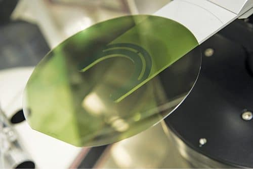
Right now, the SiC market is dominated by 10cm and 15cm wafers. Each of those are in excessive demand, however a lot of the progress is going on within the 15cm area, the place the side ratio of the wafer is 6 to 1. Whereas the business is seeking to enhance the strategies of processing for 15cm wafers, corporations are paying shut consideration to the event of 20cm SiC wafers on the identical time.
The primary cause for this transition is to cut back the appliance value of SiC. A bigger wafer dimension straight reduces the price of manufacturing. However transferring to a bigger wafer dimension just isn’t that simple and establishing mass manufacturing infrastructure takes time. As soon as the mass manufacturing of 20cm SiC is established, and the market is now not dominated by simply six to seven corporations, the price of SiC manufacturing will drop.
20cm wafers can considerably improve the manufacturing capability of SiC units since a bigger space can be utilized for manufacturing. This can be sure that extra units might be produced utilizing a single wafer of 20cm SiC. In comparison with its 15cm counterpart, 20cm wafers will nearly double the output of chip manufacturing.
Roughly twelve wafers are obtained within the batch manufacturing of 15cm and 10cm wafers. This quantity is sort of much less for 20cm wafers, which is why it’s a lot simpler to observe the single-wafer manufacturing method as an alternative of batch manufacturing. This allows us to have higher management over every wafer, in flip rising the standard of manufacturing.
As 20cm wafers grow to be a norm and manufacturing capability will increase within the coming years, we will anticipate main progress within the electrification of methods and merchandise, not simply within the automotive sector. The business would possibly slowly begin remaking some fabs that at present run on silicon with SiC expertise.
Want for unbiased processes and elevated funding prices. The manufacturing course of, in addition to the event strategy of 20cm wafers is basically completely different from 15cm wafers. Therefore, fabrication corporations should set up unbiased course of crops for the 20cm expertise, and it will add to their prices. To not point out, SiC manufacturing itself is dearer than silicon.
Danger of damages. SiC wafers are already fairly delicate. Growing a wafer of a bigger space will increase the danger of damaging the wafer throughout the substrate slicing course of. Issues like slicing stress and warpage are evident because the substrate dimension will increase.
Attaining tradeoff. Utilizing 20cm SiC will make sense provided that the advantages outweigh the challenges, most significantly when it comes to value. For instance, the effectivity of the ensuing system constructed on 20cm SiC ought to compensate for the upper SiC value in addition to the elevated prices of 20cm wafer manufacturing.
Talked about beneath are some developments which might be being witnessed at present within the silicon carbide business:
To this point, a number of SiC units have been produced and lots of have reached maturity as effectively. For instance, many corporations, together with ROHM Semiconductor, STMicroelectronics, and Infineon, have already launched a number of SiC primarily based units like MOSFETs, Schottky diodes, energy modules, and hybrid units. Additionally, many corporations are providing commercially accessible analysis kits that function modules primarily based on SiC.
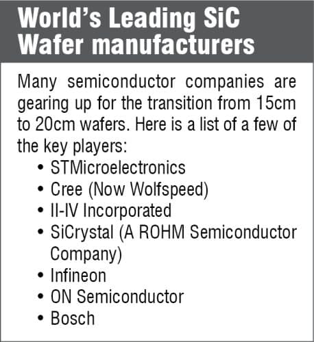
As a result of value advantages that the mass manufacturing of 20cm SiC will supply, many corporations have began the fabrication strategy of 20cm wafers. Some have already demonstrated 20cm SiC samples. These embrace Cree (now Wolfspeed), II-VI, SiCrystal (a subsidiary of ROHM Group), and STMicroelectronics.
In July 2021, STMicroelectronics introduced that it has manufactured the primary 20cm SiC bulk wafers for prototyping next-generation energy units. “The transition to 200mm SiC wafers will convey substantial benefits to our automotive and industrial clients as they speed up the transition in direction of electrification of their methods and merchandise,” says Marco Monti, President Automotive and Discrete Group, STMicroelectronics.
As a result of introduction of 5G, there can be demand for high-frequency RF energy amplifiers. That is one other potential utility business for SiC units other than the automotive sector, since GaN (gallium nitride) on SiC is a key expertise for 5G energy amplifiers. II-IV introduced in 2019 that it has launched prototype 20cm diameter semi-insulating SiC substrates for RF energy amplifiers in 5G wi-fi base-station antennas and different high-performance RF functions.
The demand for 20cm SiC is rising and lots of corporations would like to supply it in-house. Because of this they’re increasing their fabrication amenities for the mass manufacturing of 20cm wafers. A number of years down the road, we will anticipate a number of key gamers within the semiconductor enterprise to have 20cm wafer manufacturing amenities.
Bosch goals to grow to be a worldwide chief within the manufacturing of SiC chips for electromobility and plans to develop SiC units on 20cm wafers as an alternative of ordinary 15cm ones. The corporate has expanded its wafer fab amenities and is increasing even additional for full in-house manufacturing of SiC primarily based units.
Infineon has been concerned in SiC expertise for a very long time and by 2023 goals to start out mass manufacturing of 20cm SiC. Cree (Wolfspeed) plans to make use of current amenities and set up refurbished instruments to supply 20cm SiCs in a fiscally accountable method.
One other vital development on this business is the rise in investments in SiC expertise. In 2019, Cree (Wolfspeed) introduced their largest-ever funding of $1 billion to broaden SiC capability. Furthermore, collaborations and acquisitions amongst semiconductor corporations have additionally grow to be noticeable. A number of gamers from all around the world are becoming a member of the SiC race and serving to the expertise grow to be mainstream.
Many semiconductor corporations have collaborated, began joint ventures and partnerships within the SiC area. On 1st February 2022, II-VI Included introduced that it has expanded its relationship with GE by signing a three-year expertise entry settlement (TAA) with GE Analysis. In November 2021, Japanese energy electronics firm ROHM and a China primarily based agency referred to as Zhenghai Group introduced a brand new three way partnership that focuses on growing SiC energy modules for automotive functions. Many key gamers on this enterprise have invested in such partnerships with one another.
The competitors within the manufacturing of 20cm SiC is anticipated to develop, for the reason that demand for SiC is slowly rising greater than the availability. As the car business pushes SiC into the mainstream, most challenges associated to 20cm wafers talked about on this article might be eradicated. Nonetheless, it will take time, and 15cm wafers would possibly dominate the marketplace for a couple of extra years, after which the 20cm tech will take over. And when this occurs, system costs will lower significantly in comparison with 15cm SiC.
In a 2005 IEEE paper titled Silicon Carbide Energy Units – Present Developments and Potential Functions, authors Peter Friedrichsi and Roland Rupp point out the next about SiC: “The ultimate market penetration can be by some means associated to the fantasy and diploma of innovation in circuit design teams, for the reason that easy alternative of silicon by SiC alone can’t justify the price place ensuing from the implementation of SiC.”
Right now, not solely are SiC units already available in the market, we even have justifiable causes as to why 20cm SiC wafer would possibly very effectively grow to be as mainstream within the coming years as 20cm silicon wafer is in the present day.
The creator, Aaryaa Padhyegurjar, is an Business 4.0 fanatic with a eager curiosity in innovation and analysis.
[ad_2]